Save as PDF
Opens your browser print dialog — select "Save as PDF" to download.
F/2024/7151
Total Pages : 6
Second Semester
Computer Science and Engineering / Information Technology
Scheme OCBC 2019
DIGITAL TECHNIQUES
Time : Three Hours
Maximum Marks : 70
Note : i) All 7 Questions are Compulsory. Internal choices has been given in each LO (Learning Outcome).
सभी 7 प्रश्न अनिवार्य हैं। आंतरिक विकल्प प्रत्येक LO (लर्निंग आउटकम) में दिए गए हैं।
ii) In case of any doubt or dispute, the English version question should be treated as final.
किसी भी प्रकार के संदेह अथवा विवाद की स्थिति में अंग्रेजी भाषा के प्रश्न को अंतिम माना जायेगा।
1.
LO1 &
LO2
LO2
a)
Given the two binary numbers X = 1010101 and Y = 1001011, perform the subtraction X-Y using 1's complements.
दिए गए दो बाइनरी संख्याओं X = 1010101 और Y = 1001011 को, 1 के पूरक का उपयोग करके घटाव X-Y करें।
7
b)
Determine the value of base x, if (211)x = (152)8.
आधार x का मान ज्ञात कीजिये, यदि (211)x = (152)8
3
c)
Do as directed :
(2ED)16 = ( )8 = ( )2
5
OR/अथवा
a)
Explain the difference between Analog and Digital systems.
एनालॉग और डिजिटल प्रणालियों के बीच अंतर की व्याख्या कीजिए।
5
2.
LO3
a)
Why are NAND and NOR gates known as universal gates? Explain in detail with suitable example.
NAND और NOR गेट्स को यूनिवर्सल गेट के रूप में क्यों जाना जाता है? उपयुक्त उदाहरण के साथ विस्तार से समझाइए।
6
b)
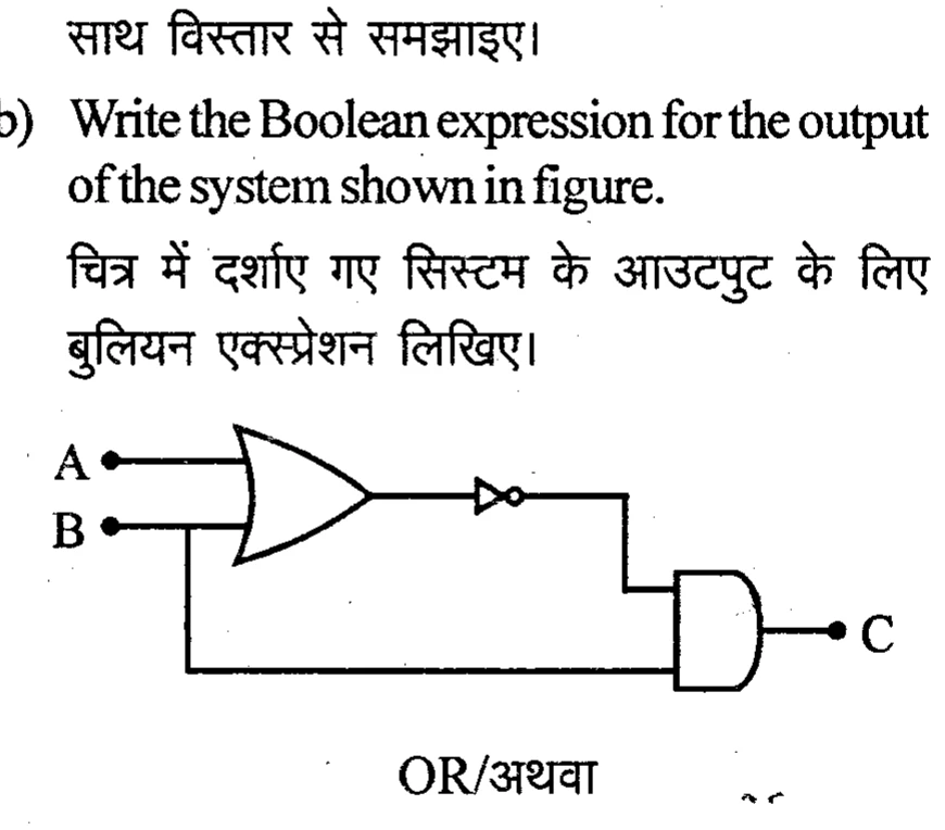
Write the Boolean expression for the output of the system shown in figure.
चित्र में दर्शाए गए सिस्टम के आउटपुट के लिए बुलियन एक्सप्रेशन लिखिए।
4
OR/अथवा
a)
Prove that a positive-logic AND gate is a negative-logic OR gate and vice-versa.
साबित करें कि एक पॉजिटिव लॉजिक AND गेट नेगेटिव लॉजिक OR गेट है और इसके विपरीत।
5
b)
Realize 2 input X-OR and X-NOR gate using NAND gates only.
केवल NAND गेट का उपयोग करके 2 इनपुट X-OR और X-NOR गेट को बनाइए।
5
3.
LO4
Simplify the following function in SOP using K-map and realise this function using NOR gates only.
F(A, B, C, D) = Σm(0, 1, 4, 5, 10, 11, 14, 15)
F(A, B, C, D) = Σm(0, 1, 4, 5, 10, 11, 14, 15)
निम्नलिखित फंक्शन को K-मैप का उपयोग करके SOP में सरल कीजिए और केवल NOR गेट्स का उपयोग करके इस फंक्शन को बनाइए।
F(A, B, C, D) = Σm(0, 1, 4, 5, 10, 11, 14, 15)
F(A, B, C, D) = Σm(0, 1, 4, 5, 10, 11, 14, 15)
10
OR/अथवा
a)
State and explain the De-Morgan's theorem.
डि-मोर्गन के प्रमेय को स��पष्ट करें और समझाइए।
4
b)
Simplify the following logical expression and realise using basic gates.
ABC + ABC + ABC + ABC
ABC + ABC + ABC + ABC
निम्नलिखित लॉजिकल समीकरण को सरल बनाइए और बेसिक गेट का उपयोग करके बनाइए।
ABC + ABC + ABC + ABC
ABC + ABC + ABC + ABC
6
4.
LO6 &
LO7
LO7
a)
Draw circuit of full subtractor and explain its working with the help of truth table.
फुल सबट्रेक्टर का सर्किट आरेखित करें और सत्यता सारणी की सहायता से इसके कार्य की व्याख्या करें।
7
b)
Mention any three applications of Multiplexers.
मल्टीप्लेक्सर के किन्हीं तीन एप्��िकेशन का उल्लेख करें।
3
OR/अथवा
a)
Draw the circuit diagram of BCD to 7-segment decoder and write its truth table.
BCD से 7-सेगमेंट डिकोडर के सर्किट डायग्राम आरेखित करें और इसकी सत्य तालिका लिखें।
7
b)
Design 4:1 multiplexer using 2:1 multiplexers.
4:1 मल्टीप्लेक्सर को 2:1 मल्टीप्लेक्सर का उपयोग कर डिजाइन करें।
3
5.
LO9 &
LO10
LO10
a)
Compare various digital logic ICs families on different parameters.
अलग-अलग मापदंडों पर विभिन्न डिजिटल लॉजिक IC परिवारों की तुलना करें।
5
b)
Draw NOR gate using ECL logic and explain it.
ECL लॉजिक का उपयोग करके NOR गेट को ड्रा करें और उसे समझाइए।
5
OR/अथवा
a)
Explain the RTL circuit with the help of circuit diagram.
सर्किट डायग्राम की सहायता से RTL सर्किट की व्याख्या कीजिए।
5
b)
Define the following characteristic parameter of digital ICs:
i) Fan out
ii) Fan in
iii) Power dissipation
iv) Propagation delay
v) Figure of merits
i) Fan out
ii) Fan in
iii) Power dissipation
iv) Propagation delay
v) Figure of merits
डिजिटल IC के निम्नलिखित विशेषता पैरामीटर को परिभाषित करें।
i) फैन आउट
ii) फैन इन
iii) पॉवर डिसिपेशन
iv) प्रोपेगेशन डिले
v) फिगर ऑफ मेरिट
i) फैन आउट
ii) फैन इन
iii) पॉवर डिसिपेशन
iv) प्रोपेगेशन डिले
v) फिगर ऑफ मेरिट
5
6.
LO11
a)
Explain the working with logic diagram of S-R flip-flop.
S-R फ्लिप-फ्लॉप के लॉजिक डायग्राम के साथ कार्य को स्पष्ट कीजिए।
6
b)
Explain briefly the concept of edge triggering in flip-flops.
फ्लिप-फ्लॉप में एज ट्रिगरिंग की अवधारणा को संक्षेप में समझाइए।
4
OR/अथवा
a)
Explain race-around condition in relation to the J-K flip-flops using timing relationships. Draw the clocked Master-Slave J-K flip-flop configuration and explain how it removes race-around conditions in J-K flip-flops?
टाइमिंग रिलेशनशिप का उपयोग करके J-K फ्लिप-फ्लॉप के संबंध में रेस-अराउंड स्थिति की व्याख्या करें। मास्टर-स्लेव J-K फ्लिप-फ्लॉप कॉन्फ़िगरेशन बनाइए और समझाइए कि यह J-K फ्लिप-फ्लॉप में रेस-अराउंड की स्थिति को कैसे दूर करता है?
7
b)
Write a short on one-bit memory cell.
एक-बिट मेमोरी सेल पर एक शॉर्ट नोट लिखें।
3
7.
LO12
a)
List out different types of shift register and explain each one with its simple diagram and waveform.
विभिन्न प्रकार के शिफ्ट रजिस्टर को सूचीबद्ध करें और प्रत्येक को अपने सरल डायग्राम और वेवफॉर्म के साथ समझाइए।
6
b)
List down the differences between synchronous and asynchronous counters.
सिंक्रोनस और एसिंक्रोनस काउंटरों के बीच अंतर सूचीबद्ध करें।
4
OR/अथवा
a)
Classify different types of Counter. Explain the ripple counter with example in details.
विभिन्न प्रकार के काउंटरों को वर्गीकृत कीजिए। रिपल काउंटर की उदाहरण के साथ व्याख्या करें।
5
b)
The initial content of a 4-bit shift register is 0110. The register is shifted 5-times to right with serial input being 10011. What will be the content of register after each shift and also draw the waveform of each shift?
एक 4-बिट शिफ्ट रजिस्टर की प्रारंभिक कंटेंट 0110 है। रजिस्टर को सीरियल इनपुट 10011 देकर 5 बार राइट शिफ्ट है। प्रत्येक शिफ्ट के बाद रजिस्टर का कंटेंट क्या होगा और वेवफॉर्म को बनाइए।
5