Save as PDF
Opens your browser print dialog — select "Save as PDF" to download.
Note: i) Attempt any five questions.
किन्हीं पाँच प्रश्नों को हल कीजिए।
ii) All questions carry equal marks.
सभी प्रश्नों के समान अंक हैं।
iii) In case of any doubt or dispute the English version question should be treated as final.
किसी भी प्रकार के संदेह अथवा विवाद की स्थिति में अंग्रेजी भाषा के प्रश्न को अंतिम माना जावेगा।
a) Explain the formation of depletion region in a PN Junction diode.
PN जंक्शन डायोड में कमी क्षेत्र के गठन को समझाइए।
b) Explain the functioning of a PN diode in both forward and reverse bias regions.
फॉरवर्ड और रिवर्स बायस दोनों क्षेत्रों में PN डायोड की कार्यप्रणाली की व्याख्या करें।
a) Explain the working and construction of MOSFET also draws its characteristics.
MOSFET की कार्यप्रणाली और निर्माण के साथ-साथ इसकी विशेषताओं को भी समझाइए।
a) Explain the operation of a tunnel diode with suitable characteristics and energy band diagrams. What is the significance of the negative resistance region?
उपयुक्त विशेषताओं और ऊर्जा बैंड आरेखों के साथ टनल डायोड के संचालन की व्याख्या करें। नकारात्मक प्रतिरोध क्षेत्र का क्या महत्व है?
b) Obtain the expression for the frequency of oscillation of an RC Phase shift oscillator.
RC चरण शिफ्ट ऑसिलेटर के दोलन की आवृत्ति के लिए अभिव्यक्ति प्राप्त करें।
a) Explain the block diagram of a 555 IC. Explain the Astable Multi-vibrator using 555 timer.
555 IC के ब्लॉक आरेख को समझाइए। 555 टाइमर का उपयोग करते एस्टेबल मल्टी-वाईब्रेटर को समझाइए।
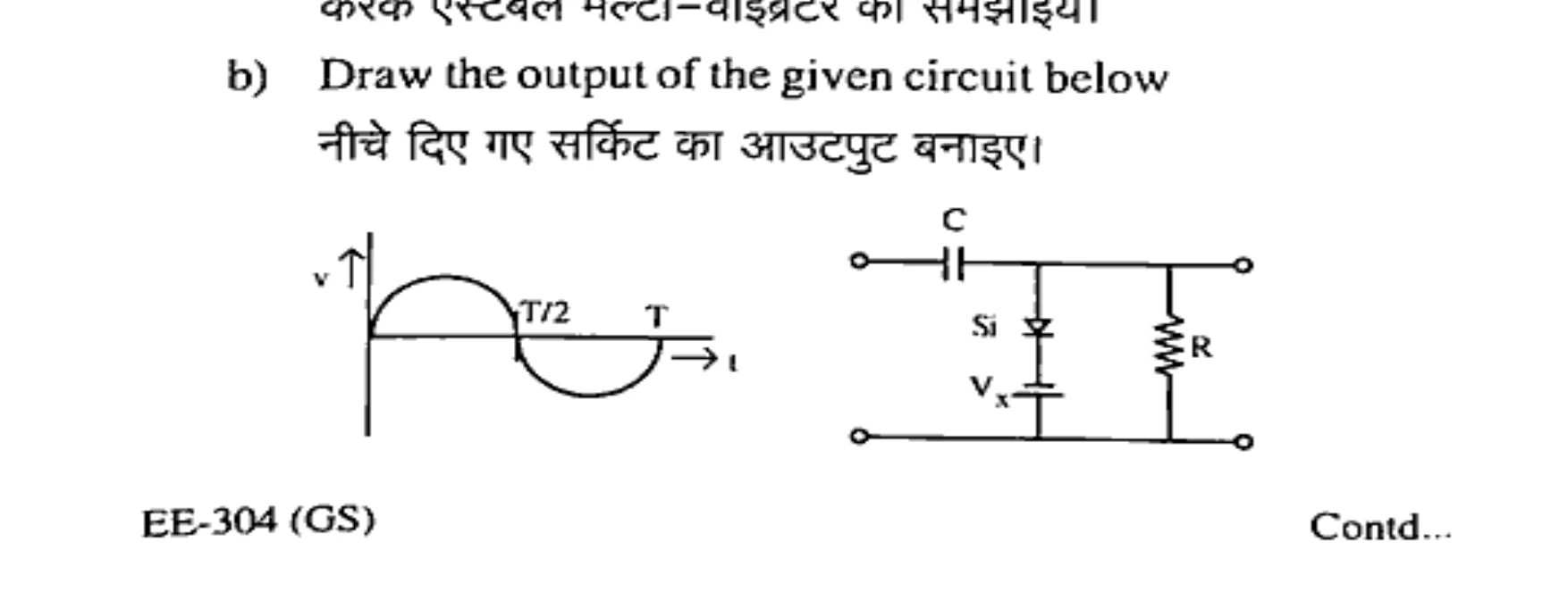
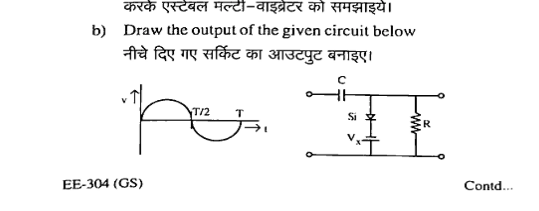
b) Draw the output of the given circuit below
नीचे दिए गए सर्किट का आउटपुट बनाइए।
a) Derive the expression for IDC and Irms for half wave rectifier circuit and find its maximum efficiency.
हाफ वेव रेक्टिफायर सर्किट के लिए IDC और Irms के लिए अभिव्यक्ति प्राप्त करें और इसकी अधिकतम दक्षता ज्ञात करें।
b) Compare briefly the half wave, centre tap full wave and bridge rectifiers.
हाफ वेव, सेंटर टैप फुल वेव और ब्रिज रेक्टिफायर की संक्षेप में तुलना करें।
a) Explain any two of the following:
- i) Log-anti log amplifiers using Op-Amp
- ii) Light Emitting Diode
- iii) Photo diode
निम्नलिखित में से किन्हीं दो की व्याख्या करें:
- i) Op-Amp का उपयोग करके लॉग-एंटी लॉग एम्प्लीफायर
- ii) प्रकाश उत्सर्जक डायोड
- iii) फोटो डायोड
b) Discuss the thermal runaway in a transistor. What is the importance of Heat Sinks?
ट्रांजिस्टर में थर्मल रनवे पर चर्चा करें। हीट सिंक का क्या महत्व है?
a) Why is a FET called voltage controlled device? What are the advantages of a MOSFET compared to a normal FET?
FET को वोल्टेज नियंत्रित उपकरण क्यों कहा जाता है? सामान्य FET की तुलना में MOSFET के क्या फायदे हैं?
a) Explain the terms :
- i) Drift and Diffusion
- ii) Zener and avalanche breakdowns
शर्तें स्पष्ट करें:
- i) बहाव और प्रसार
- ii) जेनर और हिमस्खलन ब्रेकडाउन
b) Explain the operation of Inverting, Non-inverting and Unity gain amplifiers using Op-AMPs.
Op-AMP का उपयोग करके इनवर्टिंग, नॉन-इनवर्टिंग और यूनिटी गेन एम्प्लीफायर के संचालन को समझाइए।